
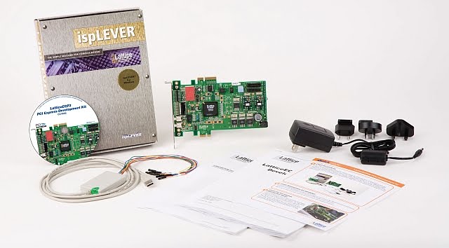
Lattice Semiconductor has developed a low cost PCI Express development kit for its LatticeECP3 family of low power FPGAs. Based on a new ECP3 PCI Express solutions board, the kit accelerates development of PCI Express designs. The kit has been developed from the ground up to accelerate the evaluation of PCI Express technology, demonstrate a range of solutions that match typical application requirements and speed users to design exploration.
“The LatticeECP3 FPGA is an excellent low power, high value programmable platform for PCI Express,” said Shakeel Peera, Lattice’s Director of Strategic Marketing for High Density Solutions. “The new LatticeECP3 PCI Express development kit will help users reduce complexity and shrink the time-to-market window for their PCI Express designs.”
The kit is an all-inclusive package optimized for creating a design with the low-power, low-cost LatticeECP3 FPGA family with a highly-optimized, low-cost PCI Express evaluation board that enables both x1 and x4 endpoint evaluation and design. There are a variety of demo executables, from a basic demo for control plane applications, throughput demo for high-bandwidth applications, color bar demo and an image transfer demo - that show how to address different design performance requirements.
The 60 day software tools license includes an x1/x4 endpoint IP core and scatter-gather DMA IP core permit users to get up and running right away and available on both Windows and Linux platforms.
The components of the LatticeECP3 PCI Express development kit have been configured to work together to enable fast system evaluation and design. With the help of easy step-by-step instructions, designers can expect to have a demo running in as little as 30 minutes, and a design validated in less than two hours.
LatticeECP3 FPGA Family
The LatticeECP3 FPGA family is five devices that offer standards-compliant multi-protocol 3.2G SERDES, DDR1/2/3 memory interfaces and high performance, cascadable DSP slices that are ideal for high performance RF, baseband and image signal processing. Toggling at 1Gbps, the LatticeECP3 FPGAs also feature the fastest LVDS I/O available in a mid-range FPGA family, as well as embedded memory of up to 6.8 Mbits. Logic density varies from 17K LUTs to 149K LUTs with up to 586 user I/O. The LatticeECP3 FPGA family is ideally suited for deployment in high volume cost- and power-sensitive wireline and wireless infrastructure applications, as well as security/surveillance, medical and industrial applications.
The development kit is available now, with a list price of $895.00. The kit can be ordered through Lattice sales or through the Lattice on-line store at http://www.latticesemi.com/
![Reblog this post [with Zemanta]](http://img.zemanta.com/reblog_e.png?x-id=db8c4403-c60e-4d77-881f-ccb7b90dcad9)
No comments:
Post a Comment